Maintenance-free, durable products
Certified quality from a single source
40 Jahre Know-How
Made in Germany

Start | Applications | Oxidation and cleaning silicon wafers
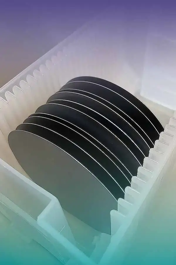
Ozone is used in the semiconductor industry for disinfection, reduction of total organic carbon (TOC) in rinsing water, wafer cleaning and Si02 formation. The sterilization ability of ozone due to its strong oxidizing power and the disruption of the bacteria’s membrane permeability is well known and has been used for the sterilization of drinking water for many years.
In the semiconductor industry, the sterilization ability is used for the disinfection of process water to reduce the formation of contaminants on tubes and for the disinfection of rinsing water to prevent defects on the wafer.
Organic contaminants in the rinsing water could also cause a haze over the wafer surface that contaminates the wafer and leads to wafer defects. The ability of ozone to reduce these organic contaminants can be enhanced by the combination of ozone and UV light called Advanced Oxidation Process (AOP), in which hydroxyl radicals are formed with a higher oxidation potential than ozone alone.
+ Reduction of the consumption of hazardous chemicals
+ Applicated in single-wafer-spin-cleaning (SCROD)
+ Saving of deionized (DI) water
+ Shorter rinsing times

+ Forming carbon dioxide and water
+ High ozone concentration and pressure
+ Significant high oxidation rate on the surface
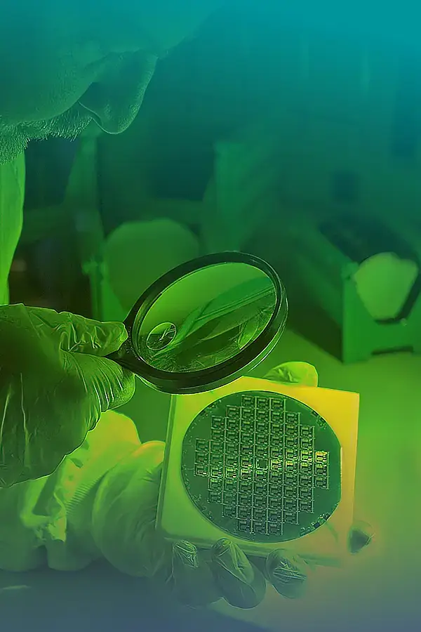
+ Metallic impurities are removed from the silicon surface
+ Cleaning process at low temperature
+ Low roughness niveau of surfaces
+ Short reaction time instead of ozone generated HCl-radicals
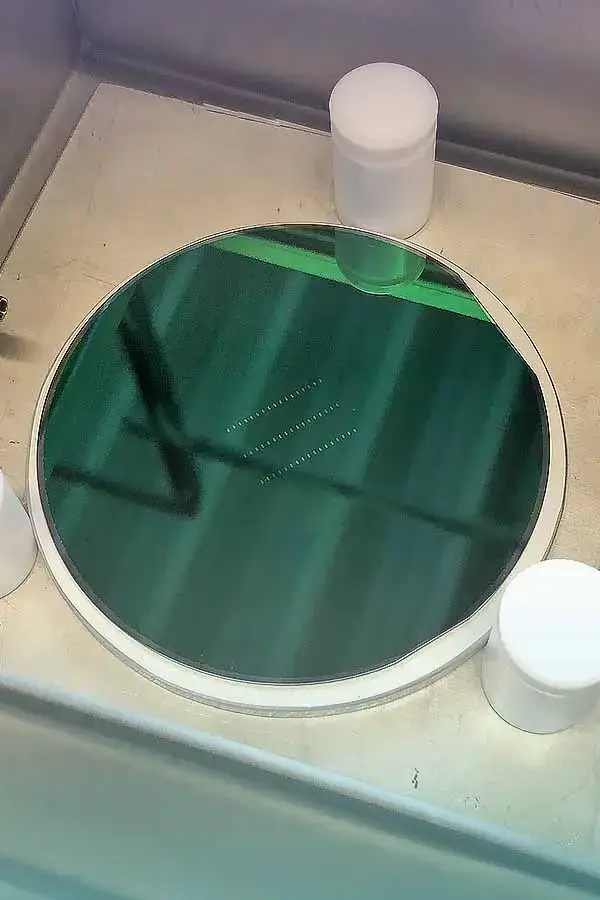
+ Strong oxidation agent for removal of organic contaminants
+ Constant ozone concentration
+ Higher standard potential than hydrogen peroxides
+ Less working temperature
+ Less consumption of energy and material
+ Reduced chemical waste
+ No reaction with metals or particles on surfaces
+ Ultra-low etching rate of wafer surfaces
+ Compatible and usable with HF- and HCl-chemicals for removing metallic and ionic contaminants from the surface
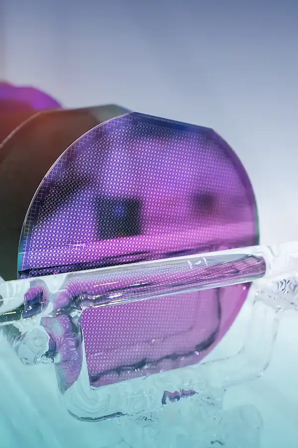
Steril processing is a important factor in production of semiconductors. Cleaning surfaces of wafers in ozone carbinets is a efficient step for clean wafer processing.
Please ask us for our steril chambers!
The main application of ozone in the semiconductor industry is wet cleaning in combination with diluted hydrofluoric acid (DHF). The main advantages compared to the traditional RCA clean are the reduction of the consumption of hazardous chemicals and the saving of deionized (DI) water due to much shorter rinsing times.The main cleaning techniques IMEC clean, the Diluted Dynamic Clean (DDC) and the Ultra Clean Technology (UCT) – all first use a combination of DI water and ozone (DI03) for the removal of organic contamination and noble metals. The following steps for the removal of particles, metals and the oxide layer are different. For example, in IMEC cleaning DI water containing hydrofluoric and hydrochloric acid is used. A hydrophobic H-stabilized surface is obtained and if desired only rinsed with DI water. If a hydrophilic surface is desired, DI03 with HCL or another ozone mixture is used to re-grow a thin oxide layer. An advancement of the DHF/DI03 based wet cleaning technique is the single-wafer spin cleaning (SCROD). DHF and DI03 are alternatively sprayed onto a rotating wafer until the wafer fits the purity requirements. In this case no impurities of other wafers can be transferred through the bath. A similar process using only DI03 can also be used for photoresist removal.
DI03 directly oxidizes the resist from the wafer surface, forming carbon dioxide and water. However, the process should take place under pressure and the ozone concentration should be as high as possible. An improvement in the ozone concentration at the wafer surface can be achieved by injecting ozone vapor into the process chamber. Ozone can diffuse through a controlled water boundary layer on the wafer surface built through the rotation, resulting in a surface ozone concentration and subsequent oxidation rates significancy higher than what can be achieved using ozone dissolved in water.
All these applications of ozone in the semiconductor industry require a high purity of ozone. Usually, ozone is generated by a high-voltage volume discharge in which the metal electrode is in contact with the tracing gas. Therefore, metal will be sputtered into the ozone gas and can contaminate the wafer surface. The high voltage electrode of a surface discharge ozone generator is generally made of tungsten, which is more resistant than the stainless steel generally used in the volume discharge generators. However, caused by the high density of energy at the electrode comers, the dielectric will be eroded over time and particle filters should be installed before using the ozone in order to avoid contamination of the wafers. To avoid fouling of the electrodes and dropping of ozone capacity in both cases additional gases must be added which remain in the process and must be degassed with the excess ozone. Solutions (from ANSEROS, for one) exist today to meet semiconductor industry requirements. Ozone can be generated in clean quartz modules without contact by the metal electrodes, and therefore no metals can contaminate the wafer surfaces. The ozone capacity remains constant with highest reliability.

